Telephone:13632750017
Cell phone:13632750017
Mail:sales@hitsemi.com
Wechat:13632750017
Pengcheng Semiconductor Technology (Shenzhen) Co., Ltd. (abbreviation: Pengcheng Semiconductor), the company is based on the intersection of the technological frontier and the market frontier, seeking innovation leadership and sustainable development, solving the pain points of the industry and localization problems, and striving for the success of the industry chain. Autonomous and controllable.
The company's core business is the research and development and manufacture of semiconductor substrate materials, the research and development and manufacture of semiconductor epitaxial wafers, and the research and development and manufacture of semiconductor process equipment. Including the R&D, manufacturing and sales of semiconductor equipment (industrial master machines); mainly PVD, CVD and MBE series equipment; R&D of hot wire CVD diamond process, design, manufacture and sales of diamond process equipment; focusing on the research and development of microcrystalline and nanocrystalline diamonds R&D and manufacturing of wafers and industrial mother machines; in the mode of industry-university-research, focusing on the second, third and fourth generation semiconductors, carry out semiconductor material preparation and research and development and pilot test of industrial mother machines, and develop and design independent and controllable complete sets Process equipment and key components, develop and design independently controllable semiconductor substrate materials and epitaxial wafers.
he company's talent team has a complete knowledge structure, and has a team of senior equipment designers from the industry. They have more than 20 years of experience in semiconductor material research, epitaxy technology research, and semiconductor thin film preparation equipment design and manufacturing.
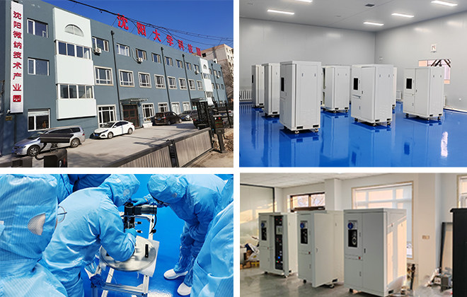
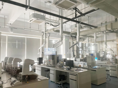
Pengcheng Semiconductor has advanced semiconductor substrate materials, semiconductor R&D equipment platform and testing equipment platform, which can carry out scientific research work from a high starting point. The company is headquartered in Nanshan District, Shenzhen City, and has a wholly-owned subsidiary in Shenyang City, which is equipped with the research and manufacturing of compound semiconductor substrate materials and epitaxial sheets, such as gallium nitride, silicon carbide, gallium oxide, etc.

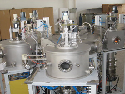
Magnetron sputtering coater, electron beam coater, thermal evaporation coater, laser deposition equipment PLD, ion beam sputter coater, magnetron and ion beam composite coater
MOCVD, PECVD, LPCVD, microwave plasma CVD, Hot silkCVD, ALD equipment
Molecular Beam Epitaxy (MBE), Laser Molecular Beam Epitaxy (LMBE)
Cluster solar thin film battery pilot line, OLED pilot equipment (G1, G2.5)
Diamond Film Preparation Equipment, Hard Coating Equipment, Magnetic Thin Film Equipment, Electrode Preparation Equipment, Alloy Annealing Furnace
DC sputtering power supply, RF radio frequency sputtering power supply, high-precision thermal evaporation power supply, high-energy DC pulse power supply (medium frequency adjustable pulse width), control system and software
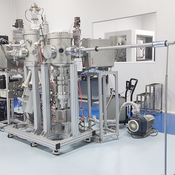
Fully self-designed and manufactured molecular beam epitaxy (MBE) equipment, including self-designed and manufactured MBE ultra-high vacuum epitaxy growth chamber, process control system and software, high temperature beam source furnace, high temperature sample stage, Rheed in-situ real-time online monitor (reflection Key components such as high-energy electron diffractometer), linear electron gun, film thickness meter (which can measure the number of molecular layers in epitaxial growth), and radio frequency source. The degree of vacuum reaches 2×10⁻⁸Pa.
The equipment was put into use in the State Key Laboratory of Optical Instruments of XX University in 2005 and is still in normal use today.
Design and manufacture a combined system of magnetron sputtering and plasma enhanced chemical vapor deposition (PECVD) technology, which is applied to the pilot line of cluster solar thin film cells. Use unit XX Institute of Electric Engineering.
Design and manufacture of diamond thin film preparation equipment, applied to research and pilot production equipment of diamond thin film materials. The current use unit is the Institute of Metal Research, XX Institute.
A fully automatic magnetron sputtering equipment is designed and manufactured, which can add horizontal and vertical magnetic fields, and a self-designed vacuum manipulator transfers the substrate. It is applied to the research and pilot test of high-density magnetic recording materials and devices. Now use the unit XX photoelectric laboratory.
Design and manufacture of OLED organic semiconductor light-emitting materials and devices research and pilot equipment. The current use unit is the Advanced Materials Laboratory of XX University.
MOCVD and alloy annealing furnaces are designed and manufactured for the epitaxial growth of GaN and ZnO, and the research and pilot test of LED inorganic semiconductor light-emitting materials and devices are realized. The current use unit is the National Silicon-based LED Engineering Technology Research Center of XX University.
Design and manufacture of OLED organic semiconductor light-emitting materials and devices research and pilot equipment. Typical users: Advanced Materials Laboratory of XX University, Jilin Allied Optoelectronic Materials Co., Ltd.
Design and manufacture of magnetron sputtering research equipment. The current use unit is the Semiconductor Institute of XX University.
Manufactured electron beam evaporator research equipment. The current use unit is XX University of Technology.
.jpg?x-oss-process=style/small)
2023
PVD epitaxial gallium nitride equipment and technology research.
2022
Preparation of large size diamond wafer (≥ φ 6 inches).
2021
MBE production design.
2019
Design and manufacture of large-scale hot filament CVD diamond film production equipment.
2017
-Optimized Rheed design, started production MBE design.
-Started to develop the process and equipment for PVD epitaxial GaN, and is currently undergoing equipment process verification.
2015 XXX Institute of Metals XX National (Joint) Laboratory Cooperation for Materials Science
Diamond epitaxy equipment was fabricated, and diamond electrodes, microcrystalline and nanocrystalline diamond films, and conductive diamond films were prepared.
2007Cooperated with XX University School of Physics
Design and manufacture of optical grade diamond growth equipment (using thermal excitation technology and CVD technology).
2006 Cooperation with XX University of Science and Technology
Design Design UHT CVD and MBE.
For 4H crystal type SiC epitaxial growth.
2005 cooperated with the State Key Laboratory of Optical Instruments of XX University
Designed and manufactured the first molecular beam epitaxy equipment with completely independent intellectual property rights for epitaxy of optoelectronic semiconductor materials.
2001 Cooperated with XX University in 2001
A pilot-scale fully automated and monitored MOCVD is designed for epitaxial GaN and ZnO.

Customer service WeChat

Wechat official account
